SEMICONDUCTORS
The elements on the "boundary" between metals and nonmetals - silicon, germanium and gallium to name the most well known, are covalent network bonded in crystals in the pure form. They are excellent insulators as pure crystals. However with traces of impurities they can be made very controllable conductors. This has been known since the 1940s as the quantum mechanics of whole crystals, as opposed to single atoms, came to be understood.
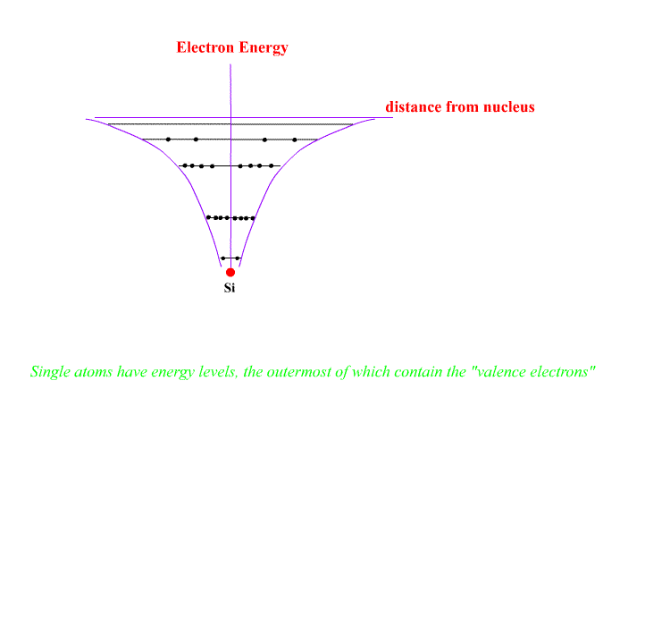
Individual atoms have energy levels holding all of the electrons. The shape of the electron energy curve with distance is of the form E ~ 1/r , hyperbolic.
"Empty" electron levels exist above the outermost electrons. Electrons may be promoted to these empty levels ion individual atoms by heating, adding light or bombarding with electrons.
The atoms may be ionised by adding energy to remove the outer electron.
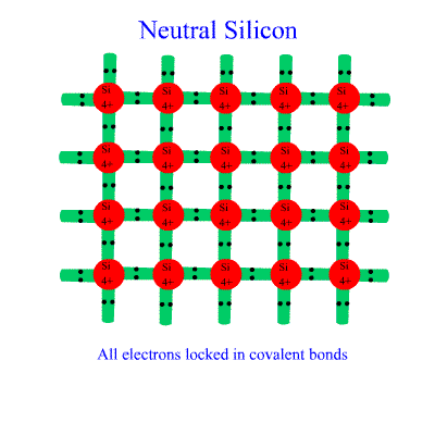
When atoms crystallise into solids, the outer electrons merge in energy and form "bonds" - covalent bonds in these cases, often "covalent-network", creating a large hard, insulating crystal. The merging atoms also merge outer energy levels to create bands in which electrons can exist. The band formed for the bonds is called the Valence Band and exists throughout the structure. Electrons in the Valence Band are at the same energy everywhere and hold the structure together. They are the electrons forming the covalent bonds.
A band further out is also formed from the higher levels - this is also right through the crystal. It is called the Conduction Band. Covalent materials have no electrons in this band unless heated or excited by some means. Metals automatically have electrons in this band - for them it is the band formed from their outer electron levels. That is why they ARE metals - the outer electrons are free to move around the whole solid in the Conduction Band.
( The reason for these bands is that electrons cannot occupy precisely the same energy levels if they have the same quantum numbers by the Pauli Exclusion Principle. Levels develop for each electron in the outer regions of the atoms and as there are about 1023 electrons in a crystal, the individual levels are effectively a band. )
Silicon and other near metals can have electrons inserted into the Conduction Band using traces of impurity atoms of similar size such as boron, phosphorus and arsenic atoms. These are close to Si etc on the Periodic Table. An example is Si with As impurities.
n-type conductors
Arsenic has one extra electron in its outer shell relative to Silicon. When introduced as a dopant, it can replace a silicon atom in the structure complete with 4 covalent electron bonds AND inject an electron into the structure loosely held to the donor by electrostatics. The arsenic atom is a donor. This electron is available for conduction with a small amount of extra energy to boost them into the Conduction Band, leaving a positively charged As atom residing in the structure. These semiconductors are called n-type for negative electron conduction.
p-type conductors
Using boron dopants, we end with a structure LACKING electrons in some places as boron has only three outer electrons. An extra electron is "borrowed" from elsewhere to make up the bond. The boron atom is called an acceptor. It will sit in the crystal as a negative charge. As the replacement can come from anywhere, the LACK of electron (a "hole") is moveable and equivalent to a mobile positive charge. This type of semiconductor is a p-type conductor. The mobile electrons are boosted into the discrete energy levels of the dopant just above the Valence band from the Valence Band to move around creating the holes in the Valence Band. The p-type "holes" move in the Valence Band.